


化工儀器網(wǎng)>產(chǎn)品展廳>光學(xué)儀器及設(shè)備>光學(xué)實(shí)驗(yàn)設(shè)備>其它光學(xué)實(shí)驗(yàn)設(shè)備> X-Ray波帶片


X-Ray波帶片
- 公司名稱(chēng) 八帆儀器設(shè)備(上海)有限公司
- 品牌 其他品牌
- 型號(hào)
- 產(chǎn)地
- 廠商性質(zhì) 經(jīng)銷(xiāo)商
- 更新時(shí)間 2021/3/22 11:52:03
- 訪問(wèn)次數(shù) 1906
聯(lián)系我們時(shí)請(qǐng)說(shuō)明是化工儀器網(wǎng)上看到的信息,謝謝!
原子力顯微鏡,,原子力拉曼,,有機(jī)合成質(zhì)譜儀,制備色譜,,納米紅外光譜儀,,掃描近場(chǎng)光學(xué)顯微鏡,電鏡下原子力,,微米級(jí)3D打印機(jī),,
| 應(yīng)用領(lǐng)域 | 綜合 |
|---|
X-Ray波帶片高質(zhì)量的X射線(xiàn)光學(xué)系統(tǒng),具有經(jīng)過(guò)驗(yàn)證的分辨率,、效率和可靠性,、低成本,,適用于ptychography,、STXM、TXM和相位對(duì)比成像的軟X射線(xiàn)和硬X射線(xiàn),。
X-Ray波帶片優(yōu)勢(shì):
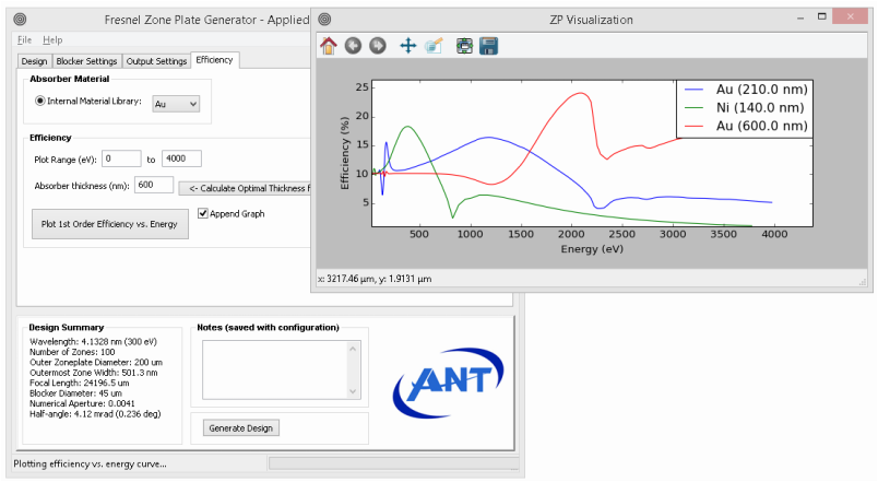
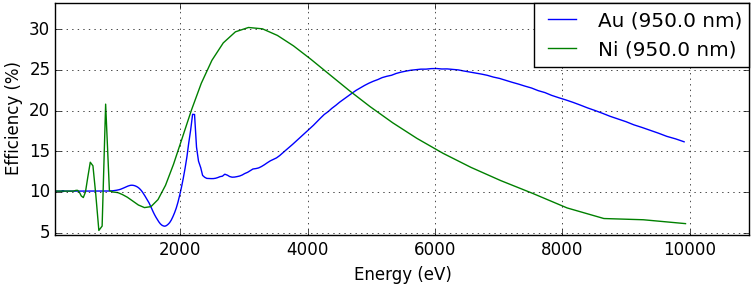 利用不同的金屬(金或鎳)可以提高一系列能量的效率,。該圖為從ANT波帶片軟件生成的圖像。
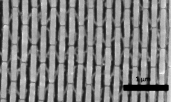
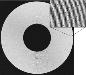 高分辨率波帶片可在大范圍的能量范圍內(nèi)提供z高的分辨率和效率,。18 nm(Δr)分辨率的波帶片提供高分辨率,,水窗效率高于20%。18 nm Au FZP圖像,,直徑270μm,,中心光闌設(shè)計(jì)。
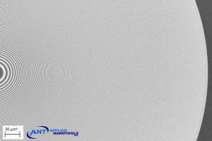 Applied Nanotool的波帶片可用于各種應(yīng)用,,包括大直徑的ptychography和幾毫米的<1 nm縫合誤差,。直徑為0.85毫米的波帶片圖像
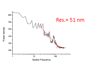 高相位對(duì)比成像,適用于分辨率為50 nm及以下的硬X射線(xiàn)應(yīng)用,。波帶片的均勻性是高相位襯度成像的關(guān)鍵組成部份,。
軟X-Ray指標(biāo)
| Device | Outer Zone Width ΔR n(nm) | Thickness (µm) | Outer Diameter (µm) | (# of zones) E/ΔE Limit | ~ Focal Length (µm) | Estimated Lead Time |
|---|---|---|---|---|---|---|
| NZP-50um-12nm | 12 | 0.05 + 0.01 | 50 | 1059 | 144 | Please Contact |
| NZP-65um-15nm | 15 | 65 | 1096 | 235 | ||
| SZP?90um?15nm | 15 | <0.1 | 90 | 1514 | 325 | 2-3 |
| SZP?120um?15nm | 120 | 2019 | 433 | |||
| SZP?200um?18nm | 18 | <0.15 | 200 | 2797 | 868 | In Stock |
| SZP?270um?18nm | 270 | 3775 | 1172 | |||
| SZP?320um?18nm | 320 | 4473 | 1389 | |||
| SZP-200um-25nm | 25 | <0.24 | 200 | 2007 | 1207 | In Stock |
| SZP?250um?25nm | 250 | 2509 | 1510 | |||
| SZP-300um-25nm | 300 | 3010 | 1811 | |||
| SZP-360um-25nm | 360 | 3612 | 2173 | |||
| TZP?160um?50nm | 50 | <0.75 | 160 | 801 | 1934 | 2 – 3 |
| TZP?280um?50nm | 280 | 1401 | 3384 | |||
| TZP?750um?200nm | 200 | <0.75 | 750 | 938 | 36292 | 1 – 3 |
| TZP?1250um?200nm | 1250 | 1563 | 60487 | |||
| *For estimated efficiency of zone plate, please see generated graphs below or download our zone plate software. | ||||||
硬X-Ray指標(biāo)
| Device | Outer Zone Width ΔR n(nm) | Thickness (µm) | Outer Diameter (µm) | (# of zones) E/ΔE Limit | Energy Range (keV) | Estimated Lead Time (months) |
|---|---|---|---|---|---|---|
| HZP-50-25nm | 25 | >0.65 | 50 | 500 | 1.5 to 10 | 2 – 3 |
| HZP-75-25nm | 75 | 750 | 2 – 3 | |||
| HZP?100um?42.5nm | 42.5 | >0.8 | 100 | 588 | 2 to 12 | 2 – 3 |
| HZP?85um?50nm | 50 | >0.9 | 85 | 425 | 2 to 12 | 2 – 3 |
| HZPX?85um?50nm | >1.7 | 5.5 to 20 | 4 – 6 | |||
| HZP?180um?50nm | >0.9 | 180 | 900 | 2 to 12 | 2 – 3 | |
| HZP?550um?50nm | >0.9 | 550 | 2750 | 2 to 12 | 2 – 3 | |
| HZPX?550um?50nm | >1.5 | 5.5 to 20 | 4 – 6 | |||
| HZP-400um-100nm | 100 | >1.2 | 400 | 1000 | 2.5 to 8 | 2 – 3 |
| HZPX?400um?100nm | >2.6 | 8 to 30 | 4 – 6 | |||
| HZP?400um?120nm | 120 | >1.5 | 400 | 834 | 5 to 25 | 2 – 3 |
| HZPX?400um?120nm | >2.6 | 8 to 30 | 4 – 5 | |||
| HZP?750um?200nm | 200 | >2.2 | 750 | 938 | 7 to 20 | 3 – 4 |
| HZPX?750um?200nm | 200 | >3.6 | 12 to 50 | 4 – 5 | ||
| *For estimated efficiency of zone plate, please see generated graphs below or download our zone plate software. All zone plate diameters can be customized for specific setups. Standard frame sizes are 3 mm x 3 mm with SiN membranes (100 nm). | ||||||
Oxide Interlock process for Hard X-Ray Optics
 Oxide Interlock process with silicon dioxide links between the gold zones, improving performance and lifetime of the zone plate optics. This comes standard on all hard X-ray optics. The silicon dioxide is highly transparent for hard X-rays.
中心光闌
中心光闌和外光闌選項(xiàng)可以顯著改善波帶板成像,降低光學(xué)器件的0次級(jí)并提高其使用壽命,。各種厚度可達(dá)3μm的芯片可用或大于10μm作為單獨(dú)的芯片,。 高分辨率18 nm外區(qū)菲涅耳波帶片頂部電鍍4μm厚中心止點(diǎn)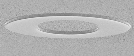 4 um thick central stop electroplated on top of Fresnel zone plate with high resolution 18 nm outer zones
Custom Designs and Frame Size
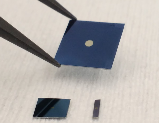 Custom silicon nitride, silicon carbide or silicon membranes down to 0.9 mm half dimensions. Image above showing 1 cm x 1 cm (top), 5 mm x 5 mm (bottom left) and 0.9 mm x 5 mm chips.
XY Stage for Zone Plates/Central Stop Alignment
Our custom XY stage allows micro-scale alignment of a central stop and zone plate and also allows for a possible blast-shield to be mounted. XY micrometer scale stage holder for central stop and zone plate alignment with blast shield<iframe allowfullscreen="true" frameborder="0" height="480" mozallowfullscreen="true" src="https://myhub.autodesk360.com/ue2c055fb/shares/public/SHabee1QT1a327cf2b7a3d447e23386eab43?mode=embed" style="box-sizing: border-box; margin: 0px; padding: 0px; border-width: 0px; border-style: initial; font-style: inherit; font-variant: inherit; font-weight: inherit; font-stretch: inherit; font-size: inherit; line-height: inherit; font-family: inherit;" webkitallowfullscreen="true" width="640">
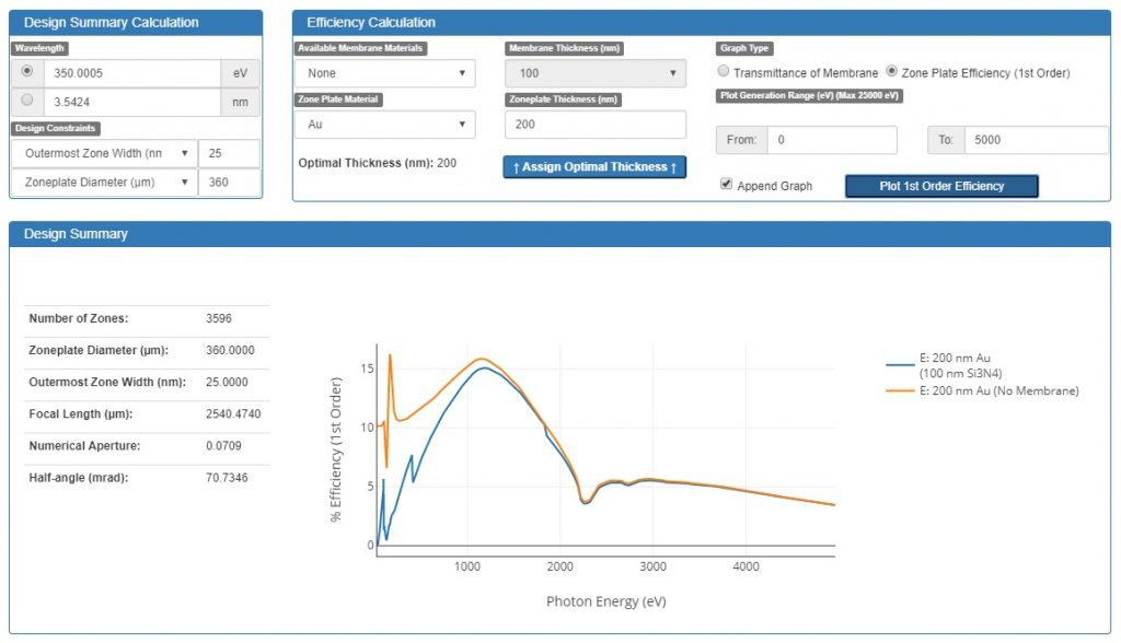
波帶片計(jì)算器
優(yōu)勢(shì)
利用不同的金屬(金或鎳)可以提高一系列能量的效率。該圖為從ANT波帶片軟件生成的圖像,。 高分辨率波帶片可在大范圍的能量范圍內(nèi)提供高的分辨率和效率,。18 nm(Δr)分辨率的波帶片提供高分辨率,水窗效率高于20%,。18 nm Au FZP圖像,,直徑270μm,中心光闌設(shè)計(jì),。 Applied Nanotool的波帶片可用于各種應(yīng)用,,包括大直徑的ptychography和幾毫米的<1 nm縫合誤差。直徑為0.85毫米的波帶片圖像 高相位對(duì)比成像,,適用于分辨率為50 nm及以下的硬X射線(xiàn)應(yīng)用,。波帶片的均勻性是高相位襯度成像的關(guān)鍵組成部份。軟X-Ray指標(biāo)
| Device | Outer Zone Width ΔR n(nm) | Thickness (µm) | Outer Diameter (µm) | (# of zones) E/ΔE Limit | ~ Focal Length (µm) | Estimated Lead Time |
|---|---|---|---|---|---|---|
| NZP-50um-12nm | 12 | 0.05 + 0.01 | 50 | 1059 | 144 | Please Contact |
| NZP-65um-15nm | 15 | 65 | 1096 | 235 | ||
| SZP?90um?15nm | 15 | <0.1 | 90 | 1514 | 325 | 2-3 |
| SZP?120um?15nm | 120 | 2019 | 433 | |||
| SZP?200um?18nm | 18 | <0.15 | 200 | 2797 | 868 | In Stock |
| SZP?270um?18nm | 270 | 3775 | 1172 | |||
| SZP?320um?18nm | 320 | 4473 | 1389 | |||
| SZP-200um-25nm | 25 | <0.24 | 200 | 2007 | 1207 | In Stock |
| SZP?250um?25nm | 250 | 2509 | 1510 | |||
| SZP-300um-25nm | 300 | 3010 | 1811 | |||
| SZP-360um-25nm | 360 | 3612 | 2173 | |||
| TZP?160um?50nm | 50 | <0.75 | 160 | 801 | 1934 | 2 – 3 |
| TZP?280um?50nm | 280 | 1401 | 3384 | |||
| TZP?750um?200nm | 200 | <0.75 | 750 | 938 | 36292 | 1 – 3 |
| TZP?1250um?200nm | 1250 | 1563 | 60487 | |||
| *For estimated efficiency of zone plate, please see generated graphs below or download our zone plate software. | ||||||
硬X-Ray指標(biāo)
| Device | Outer Zone Width ΔR n(nm) | Thickness (µm) | Outer Diameter (µm) | (# of zones) E/ΔE Limit | Energy Range (keV) | Estimated Lead Time (months) |
|---|---|---|---|---|---|---|
| HZP-50-25nm | 25 | >0.65 | 50 | 500 | 1.5 to 10 | 2 – 3 |
| HZP-75-25nm | 75 | 750 | 2 – 3 | |||
| HZP?100um?42.5nm | 42.5 | >0.8 | 100 | 588 | 2 to 12 | 2 – 3 |
| HZP?85um?50nm | 50 | >0.9 | 85 | 425 | 2 to 12 | 2 – 3 |
| HZPX?85um?50nm | >1.7 | 5.5 to 20 | 4 – 6 | |||
| HZP?180um?50nm | >0.9 | 180 | 900 | 2 to 12 | 2 – 3 | |
| HZP?550um?50nm | >0.9 | 550 | 2750 | 2 to 12 | 2 – 3 | |
| HZPX?550um?50nm | >1.5 | 5.5 to 20 | 4 – 6 | |||
| HZP-400um-100nm | 100 | >1.2 | 400 | 1000 | 2.5 to 8 | 2 – 3 |
| HZPX?400um?100nm | >2.6 | 8 to 30 | 4 – 6 | |||
| HZP?400um?120nm | 120 | >1.5 | 400 | 834 | 5 to 25 | 2 – 3 |
| HZPX?400um?120nm | >2.6 | 8 to 30 | 4 – 5 | |||
| HZP?750um?200nm | 200 | >2.2 | 750 | 938 | 7 to 20 | 3 – 4 |
| HZPX?750um?200nm | 200 | >3.6 | 12 to 50 | 4 – 5 | ||
| *For estimated efficiency of zone plate, please see generated graphs below or download our zone plate software. All zone plate diameters can be customized for specific setups. Standard frame sizes are 3 mm x 3 mm with SiN membranes (100 nm). | ||||||
Oxide Interlock process for Hard X-Ray Optics
Oxide Interlock process with silicon dioxide links between the gold zones, improving performance and lifetime of the zone plate optics. This comes standard on all hard X-ray optics. The silicon dioxide is highly transparent for hard X-rays.中心光闌
中心光闌和外光闌選項(xiàng)可以顯著改善波帶板成像,,降低光學(xué)器件的0次級(jí)并提高其使用壽命。各種厚度可達(dá)3μm的芯片可用或大于10μm作為單獨(dú)的芯片,。 高分辨率18 nm外區(qū)菲涅耳波帶片頂部電鍍4μm厚中心止點(diǎn) 4 um thick central stop electroplated on top of Fresnel zone plate with high resolution 18 nm outer zonesCustom Designs and Frame Size
Custom silicon nitride, silicon carbide or silicon membranes down to 0.9 mm half dimensions. Image above showing 1 cm x 1 cm (top), 5 mm x 5 mm (bottom left) and 0.9 mm x 5 mm chips.XY Stage for Zone Plates/Central Stop Alignment
Our custom XY stage allows micro-scale alignment of a central stop and zone plate and also allows for a possible blast-shield to be mounted. XY micrometer scale stage holder for central stop and zone plate alignment with blast shield<iframe allowfullscreen="true" frameborder="0" height="480" mozallowfullscreen="true" src="https://myhub.autodesk360.com/ue2c055fb/shares/public/SHabee1QT1a327cf2b7a3d447e23386eab43?mode=embed" style="box-sizing: border-box; margin: 0px; padding: 0px; border-width: 0px; border-style: initial; font-style: inherit; font-variant: inherit; font-weight: inherit; font-stretch: inherit; font-size: inherit; line-height: inherit; font-family: inherit;" webkitallowfullscreen="true" width="640">
波帶片計(jì)算器


 采購(gòu)中心
 化工儀器網(wǎng)