
您好, 歡迎來(lái)到化工儀器網(wǎng),! 登錄| 免費(fèi)注冊(cè)| 產(chǎn)品展廳| 收藏商鋪|
您好, 歡迎來(lái)到化工儀器網(wǎng),! 登錄| 免費(fèi)注冊(cè)| 產(chǎn)品展廳| 收藏商鋪|

13651969369
當(dāng)前位置:泰州巨納新能源有限公司>>二維材料>>硒化物晶體>> TiSe2 二硒化鈦晶體


產(chǎn)品型號(hào)
品 牌2D Semiconductors
廠商性質(zhì)生產(chǎn)商
所 在 地泰州市
更新時(shí)間:2024-06-03 09:41:38瀏覽次數(shù):808次
聯(lián)系我時(shí),,請(qǐng)告知來(lái)自 化工儀器網(wǎng)
GaTe 碲化鎵晶體 (Gallium Telluride)


| 供貨周期 | 現(xiàn)貨 | 應(yīng)用領(lǐng)域 | 環(huán)保,化工,能源,綜合 |
|---|
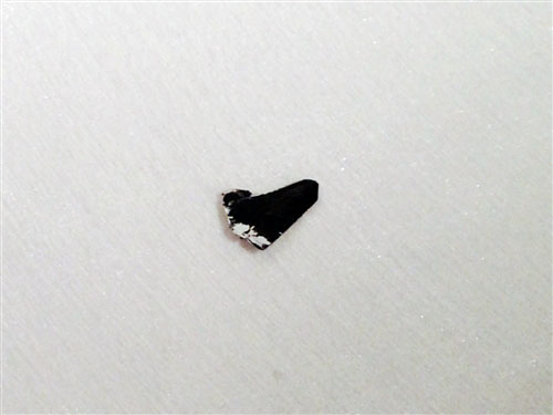
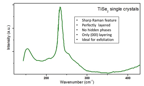
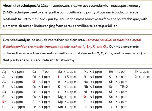
Our TiSe2 crystals are stabilized in 2H-phase (CDW metallic phase). They are grown using two different techniques through chemical vapor transport (CVT) or flux zone growth (see description of these two methods below). These crystals are treated as gold standards in 2D materials field owing to perfected electronic behavior with guaranteed CDW response. Our TiSe2 crystals are notoriously known low impurity resistance (zero temperature resistance), high carrier mobility, extremely clean and sharp XRD peaks, and negligible amount of defects (see published results as well as CVT vs. Flux based methods below ). Our TiSe2 crystals are large in size and ready for exfoliation without any preparation. If you research needs STM grade surfaces or even STM samples (TiSe2 mounted on conductive STM holders) please contact us, we will be happy to arrange these samples.
Properties of vdW TiSe2 crystals
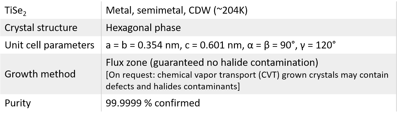
Growth method matters> Flux zone or CVT growth method? Contamination of halides and point defects in layered crystals are well known cause for their reduced electronic mobility, reduced anisotropic response, poor e-h recombination, low-PL emission, and lower optical absorption. Flux zone technique is a halide free technique used for synthesizing truly semiconductor grade vdW crystals. This method distinguishes itself from chemical vapor transport (CVT) technique in the following regard: CVT is a quick (~2 weeks) growth method but exhibits poor crystalline quality and the defect concentration reaches to 1E11 to 1E12 cm-2 range. In contrast, flux method takes long (~3 months) growth time, but ensures slow crystallization for perfect atomic structuring, and impurity free crystal growth with defect concentration as low as 1E9 - 1E10 cm-2. During check out just state which type of growth process is preferred. Unless otherwise stated, 2Dsemiconductors ships Flux zone crystals as a default choice.

請(qǐng)輸入賬號(hào)
請(qǐng)輸入密碼
請(qǐng)輸驗(yàn)證碼
以上信息由企業(yè)自行提供,信息內(nèi)容的真實(shí)性,、準(zhǔn)確性和合法性由相關(guān)企業(yè)負(fù)責(zé),,化工儀器網(wǎng)對(duì)此不承擔(dān)任何保證責(zé)任。
溫馨提示:為規(guī)避購(gòu)買風(fēng)險(xiǎn),,建議您在購(gòu)買產(chǎn)品前務(wù)必確認(rèn)供應(yīng)商資質(zhì)及產(chǎn)品質(zhì)量,。


 化工儀器網(wǎng)